5 V expansion-board supply
To supply an expansion-board module at 5 V, execute this setting at the very start of the program. After configuration, only P8/P9 can output 5 V; other I/O outputs are limited to 3.3 V.
*(volatile int*)0x40080124 = 0x1d;
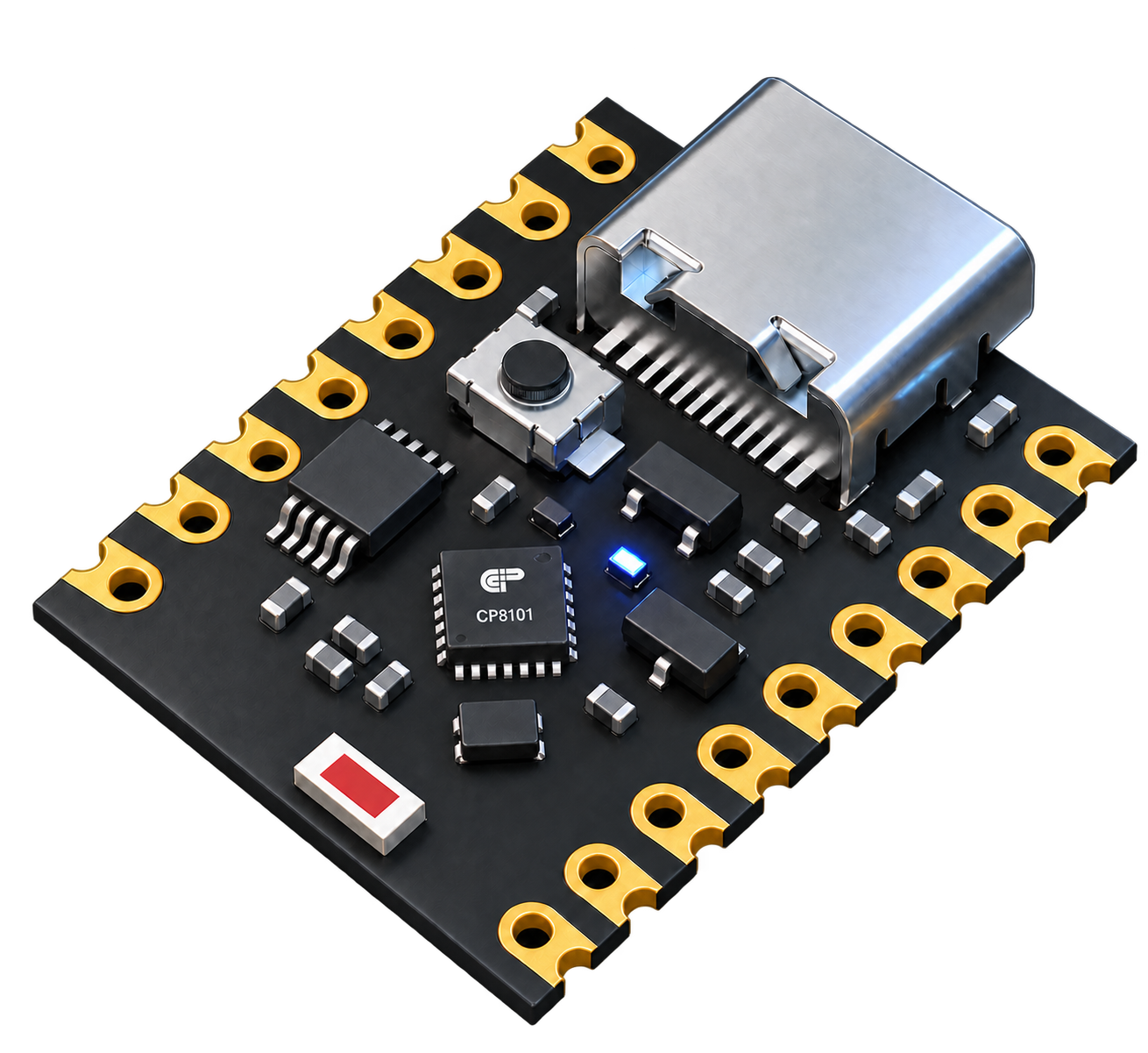
Source: CP8101 Datasheet v1.0.4, pages 2–3, 7 and 11–12. These are chip data, not CP81-MINI board measurements.
Pin names and physical order follow the supplied board photos. UART, PWM, I²C, ADC, SPI and voltage notes follow the RD pin-definition diagram supplied on 2026-09-21. The outlined front and back illustrations derive from STEP V1.0.3 geometry.
Both views place USB-C at the top. The front is the component side; the left and right rows swap when the board is viewed from underneath. Table positions 1–9 count down from the USB end and are geometric positions, not JP1/JP2 schematic pin numbers.
On phones, swipe sideways to see every pin; tap an image to open it full size.
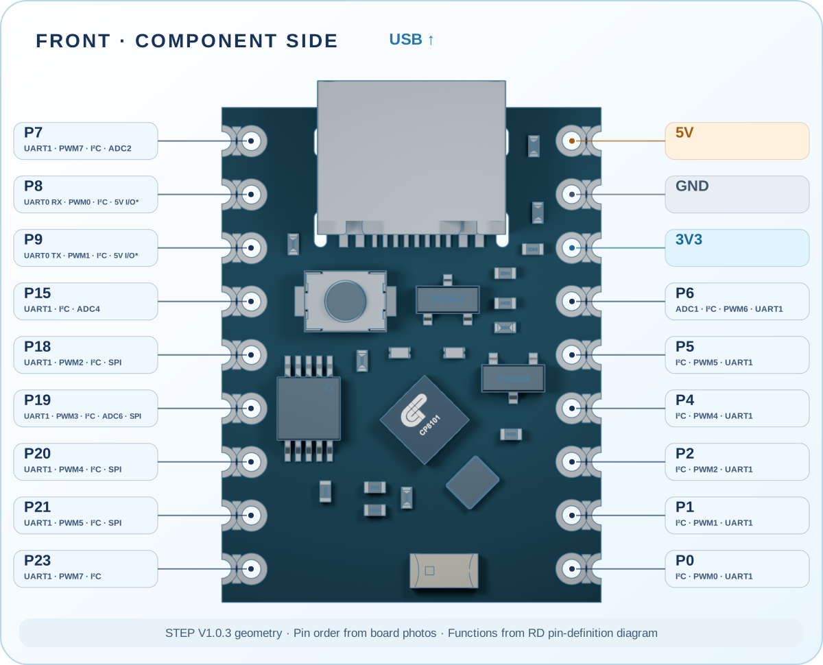
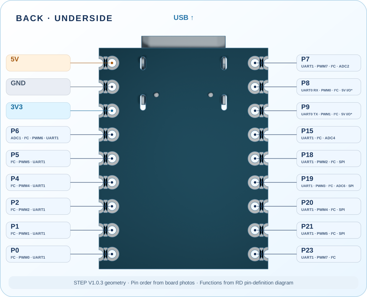
The diagram and table list every UART, PWM, I²C, ADC and SPI alternate function shown in the RD pin-definition diagram. I²C indicates an available multiplexed function and does not assign SDA or SCL; firmware selects the role and initialization. P8/P9 marked 5V I/O* must follow the setup and voltage restrictions below.
The following is transcribed from the RD screenshot supplied on 2026-09-21. Register writes and 5 V operation must be limited to the corresponding hardware and SDK revision; verify the peripheral and supply before wiring.
To supply an expansion-board module at 5 V, execute this setting at the very start of the program. After configuration, only P8/P9 can output 5 V; other I/O outputs are limited to 3.3 V.
*(volatile int*)0x40080124 = 0x1d;When I²C communication requires 5 V signaling, use only P8/P9. The RD note identifies P8/P9 as the only 5 V I/O.
P0 has one transition at power-up. For P23, RD instructs clearing bit[12] of 0x4008000C.
*(volatile int *)(0x4008000C) &= ~(1<<12);The 18 holes and outline come from STEP. Metallic contact color and the front-chip logo/CP8101 marking are visual treatments; STEP does not include actual underside traces or silkscreen. Alternate functions and voltage notes come from the RD pin-definition diagram; the website team has not yet completed per-pin electrical and firmware validation.
| Position from USB | Front leftRD alternate functions | Front rightRD alternate functions |
|---|---|---|
| 1 | P7UART1 · PWM7 · I²C · ADC2 | 5V |
| 2 | P8UART0 RX · PWM0 · I²C · 5V I/O* | GND |
| 3 | P9UART0 TX · PWM1 · I²C · 5V I/O* | 3V3 |
| 4 | P15UART1 · I²C · ADC4 | P6ADC1 · I²C · PWM6 · UART1 |
| 5 | P18UART1 · PWM2 · I²C · SPI | P5I²C · PWM5 · UART1 |
| 6 | P19UART1 · PWM3 · I²C · ADC6 · SPI | P4I²C · PWM4 · UART1 |
| 7 | P20UART1 · PWM4 · I²C · SPI | P2I²C · PWM2 · UART1 |
| 8 | P21UART1 · PWM5 · I²C · SPI | P1I²C · PWM1 · UART1 |
| 9 | P23UART1 · PWM7 · I²C | P0I²C · PWM0 · UART1 |
5V, 3V3 and GND are the 5 V supply contact, 3.3 V supply contact and ground reference. RD further states that P8/P9 can operate as 5 V I/O after the specified register setup; other GPIO outputs are limited to 3.3 V. This does not make every GPIO 5 V tolerant. Available current, protection and power direction still require a board specification.