
Updated: 2026-09-20
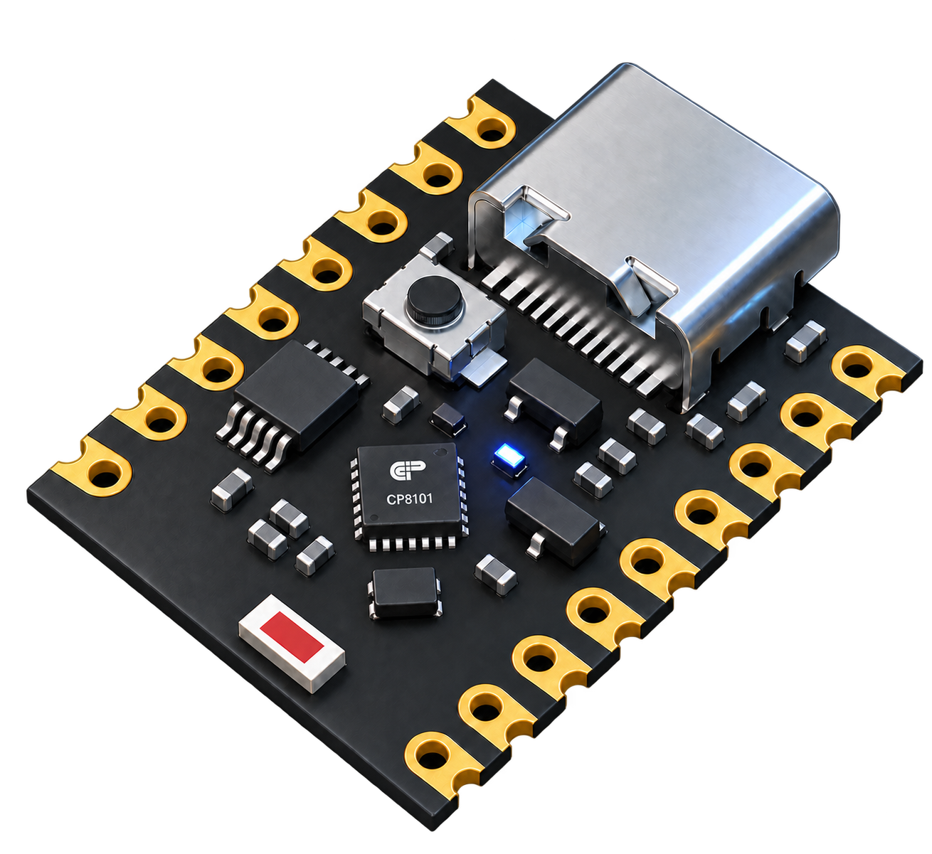
This article summarizes the CP8101 chip datasheet. Chip capability does not establish that a feature is routed, enabled or validated on the CP81-MINI board. Source: user-provided CP8101 Datasheet v1.0.4.
Core, memory and radio (pages 2–3, 7)
- 32-bit RISC-V processor up to 48 MHz; 16 KB SRAM, 64 KB ROM, 16 KB OTP and 4 KB instruction cache.
- The chip supports Bluetooth LE 5.3 and a proprietary 2.4 GHz protocol. RF table 3-5 lists 2,400–2,483.5 MHz.
- The datasheet lists up to 15 GPIO, 2 UART, 2 SPI, 1 I²C, QSPI, a 10-bit ADC, hardware AES-128 and QFN20 packaging. Its model table lists CP8101-QA23; the part populated on the board is unconfirmed.
- Flash size remains unconfirmed: page 2 describes optional 256 KB external Flash, while the page 7 model table says “2M FLASH” without a clear unit or board population detail.
Datasheet conditions (pages 2, 10–12)
Recommended chip VDD is 1.8–5.5 V. The feature list says using 5.5 V requires software configuration. Chip operating temperature is -40 to +105 °C. These figures are not board input ratings and do not authorize applying 5.5 V to a header.
The RF table lists -25 to +12 dBm TX power and typical -98.2 dBm RX sensitivity at 1 Mbps and 0.1% BER. RF figures were measured in conducted mode; antenna, PCB and firmware affect board performance. The feature list also gives 1 μA sleep, 10 μA BLE connection maintenance at a 1 s interval, 4.5 mA Rx peak @ DCDC (1 Mbps), and 5.0 mA Tx peak @ DCDC (0 dBm). These are not whole-board currents.
QFN20 chip GPIO multiplexing (pages 8–9)
These are package pin numbers and datasheet alternate functions, not a guarantee that every function is available on a CP81-MINI header. The board JP1/JP2 labels are listed separately on the specifications page and await current board verification.
| GPIO | QFN20 pin | Datasheet alternate functions |
|---|---|---|
| P0 | 5 | PWM0 / SWD_TCLK |
| P1 | 6 | PWM1 / SWD_TMS |
| P2 | 7 | PWM2 |
| P4 | 8 | PWM4 |
| P5 | 9 | PWM5 / SPI_SCK |
| P6 | 10 | PWM6 / SPI_MOSI / ADC1 |
| P7 | 11 | PWM7 / SPI_MISO / ADC2 |
| P8 | 12 | PWM0 / SPI_NCS / UART0_Rx |
| P9 | 13 | PWM1 / SPI_SCK / UART0_Tx |
| P15 | 14 | ADC4 |
| P18 | 15 | PWM2 / SPI_MOSI |
| P19 | 16 | PWM3 / SPI_MISO / ADC6 |
| P20 | 17 | PWM4 / SPI_NCS |
| P21 | 18 | PWM5 |
| P23 | 19 | PWM7 / BUCK_EN |
Board validation still needed
Header electrical ratings, RF antenna and approvals, populated Flash, power input, firmware support and programming flow require updated board material or physical validation. The earlier schematic V1.0.2 is used only for external JP1/JP2 I/O labels; its other circuits have changed and are excluded here.